The Evolution of Printed Circuit Boards
Did you know that electronic devices have a “nervous system”? That’s right – a sturdy, flat piece of plastic or fiberglass called a Printed Circuit Board (PCB). PCBs hold and connect various electronic components, like resistors, capacitors and microchips and are found in electronic gadgets from smartphones and computers to TVs and cars.
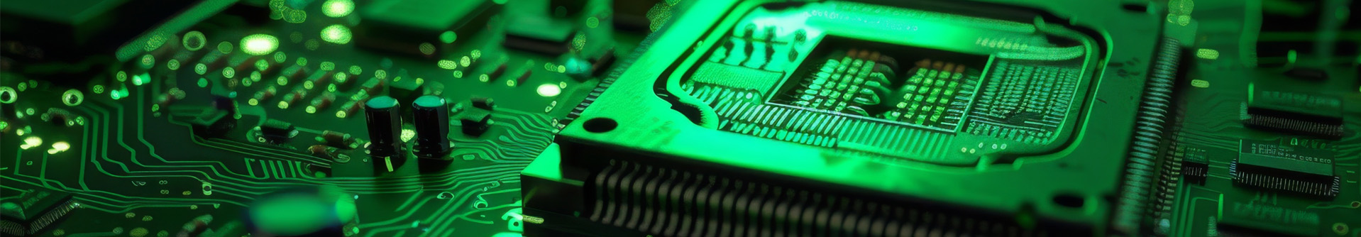
PCBs are made of thin, flat lines of metal (usually copper) that act like wires allowing electricity to flow between components making a device work. However, the definition and types of PCBs vary from single to double and multi-layer designs with corresponding copper layers. The highest-density PCBs consist of multiple layers with plated holes that connect conductors. And extra firm PCBs consist of a substrate made from FR-4 glass epoxy.
The history and evolution of Printed Circuit Boards (PCBs) is a fascinating journey that highlights their significant impact on modern history. From their early conception to their widespread use today, PCBs have transformed the landscape of electronic devices and systems.
How Conflict Fueled PCB Growth
The evolution of PCBs has been significantly influenced by historical milestones, particularly during periods of conflict. These pivotal turning points drove rapid advancements and shaped the technology we rely on today.
Early Developments (1850-1900)
The foundation for PCBs was laid in the late 19th century when electricity began powering cities and homes. Innovations like the telephone, light bulb and consumer cameras emerged setting the stage for more advanced electrical devices.
The Kitting Experts
From complete BOM to consigned and turnkey kits, we are the premier shop, with more than 60 years combined knowledge in the electronics components field.
DETAILSInitial Inventions (1900-1950)
In 1903, Albert Hanson, a German inventor filed the first patent for a PCB-like device designed for telephone systems. This early version contained conductors on both sides of an insulating board, similar to modern PCBs. A precursor to modern PCBs, in 1927 Charles Ducas patented a method for printing electronic pathways onto a board.
However, it wasn’t until World War II when PCB development significantly accelerated. The United States and its allies recognized the strategic importance of electronics in warfare. This recognition drove investment in research and development, leading to the creation of more sophisticated and reliable PCBs.
British and American military forces adopted PCB technology for devices like the proximity fuse which allowed artillery to hit precise targets, as well as military communications, radar systems and other critical technologies. Austrian inventor Paul Eisler, who fled to England to escape Nazi persecution, advanced PCB design by using copper foil on a non-conductive base, a method still used today.
Post-War Expansion (1950-2000)
After WWII PCBs became more prevalent. In 1947 Bell Labs introduced the transistor which revolutionized electronic communication. By the 1950s the U.S. Army had patented a method for assembling electrical circuits, laying the groundwork for modern PCBs.
While the 1950s witnessed a boom in the production of electronic devices, from televisions and radios to early computers, the space race of the 1960s spurred significant post-war growth and further advancements. The need for lightweight, efficient components made PCBs ideal for spacecraft. Innovations like plated through-hole technology and surface mount technology allowed for more compact and reliable designs.
During the 1970s and 1980s, however, PCBs became essential in consumer electronics, from home computers to gaming consoles. The development of the microprocessor by Texas Instruments’ Jack Kilby marked another leap forward. By the 1990s, as the internet became widespread, PCBs enabled the creation of smaller, more powerful devices including cell phones and personal computers.
Materials Management
We store your materials in a climate-controlled and ESD stockroom with a segregated customer inventory area. No extra or hidden fees for handling or BOM changes.
DETAILSThe Modern Era (2000 and Beyond)
In the 21st century, PCBs are integral to virtually every electronic device. Innovations have made it possible to integrate numerous functions into single, compact units like smartphones and tablets. PCBs will continue to evolve, potentially powering smart homes, driverless cars and advanced robotics.
We Aren’t Done Yet
Looking ahead, the future of PCBs is filled with exciting possibilities. The miniaturization of PCBs remains a key focus as technology continues to advance. The trend towards smaller, more powerful electronic devices necessitates the development of increasingly compact and efficient PCBs. Innovations in materials and manufacturing techniques are driving this miniaturization, enabling the creation of devices that were once thought impossible.
At United Pacific Electronics, we are at the forefront of this innovation. From BOM Kitting to materials management we streamline the manufacturing process and ensure the highest quality standards. Make us your trusted partner in PCB production today.
How We’re Unique
UPE’s streamlined process allows us to work “outside the box” to offer quality production for projects of any size — from the smallest to the largest run.
DETAILS